Electronic and Optoelectronic Devices based on Low-Dimensional Materials
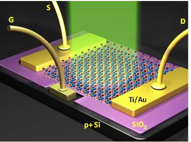
The ultra-thinness and flexibility endue the low-dimensional materials the great advantages in electronics and optoelectronics. The flexibility and stability make them superb for wearable and implantable devices with the potentials in biological, medical, and environmental applications, as well as consumer electronics. The ultra-thinness further pushes the application of the low-dimensional materials to the quantum limit. The atomic-level thickness facilitates strong coupling with the optical evanescent wave, make the low-dimensional material the ideal platform for the application of near-field optics, photonics, and optoelectronics. Our lab is aiming to fully explore these potentials to further advance the development of modern electronics and optoelectronics for both fundamental research and actual applications.
Surface/Interfacial Science and Engineering of Quantum Materials
The emerging quantum materials enable a bottom-up strategy for complex system design and engineering with rich physics properties and significant potentials in quantum computing and sensing. The surfaces and interfaces play an essential role in determining the interaction among the building blocks and the functions of the system. Realizing the importance of the surfaces and interfaces, Lei groups is making great efforts in investigating the nature and controlling methods of them, in order to tailor the properties of these quantum materials for improved performances. Our methods include physical adatom deposition, chemical treatment, epitaxial growth, etc. Supported by our state-of-the-art instruments, we are able to determine the effects of the surface/interfacial states on the lattice structure, photon response, lateral transport, quantum tunneling and so forth.


